Device to Read Micro Sd Card Circuit
Interfacing Microcontrollers with SD Card
The secure digital card (SD) is a depression price, non-volatile memory card format developed by the SD Card Association. Since its inception back at the showtime of the century, the demand for this medium-sized, free energy and space-efficient, the memory storage device has been growing at a fast rate. Therefore, to meet the marketplace requirements, the SDA was set up as a non-profit organization to promote and create SD Carte du jour standards. There are various topics related to the SD card such every bit the unlike device families, speed classes, smart cards, card security and so on and it is used in various markets like digital cameras, personal computers, and embedded systems. Some of the standard variations include SD, SDHC, SDXC, SD-ultra loftier speed etc. The microSD is the miniaturized SD memory menu format with a modest course factor and is widely used in various electronic devices.
What we are going to learn is the use of SD cards in an embedded arrangement. To exist specific, we will be dealing with the employ of SD cards in small embedded systems.
Circuit and Interfacing
SD card has a native host interface autonomously from the SPI mode for communicating with primary devices. The native interface uses four lines for data transfer where the microcontroller has SD card controller module and it needs separate license to use it. Since the SPI is a widely used protocol and it is bachelor in most low-cost microcontrollers, the SPI mode is the widely used interface in low cost embedded systems. The working voltage range of SD family is 2.7V to 3.6V and this is indicated in the operation status register (OCR).
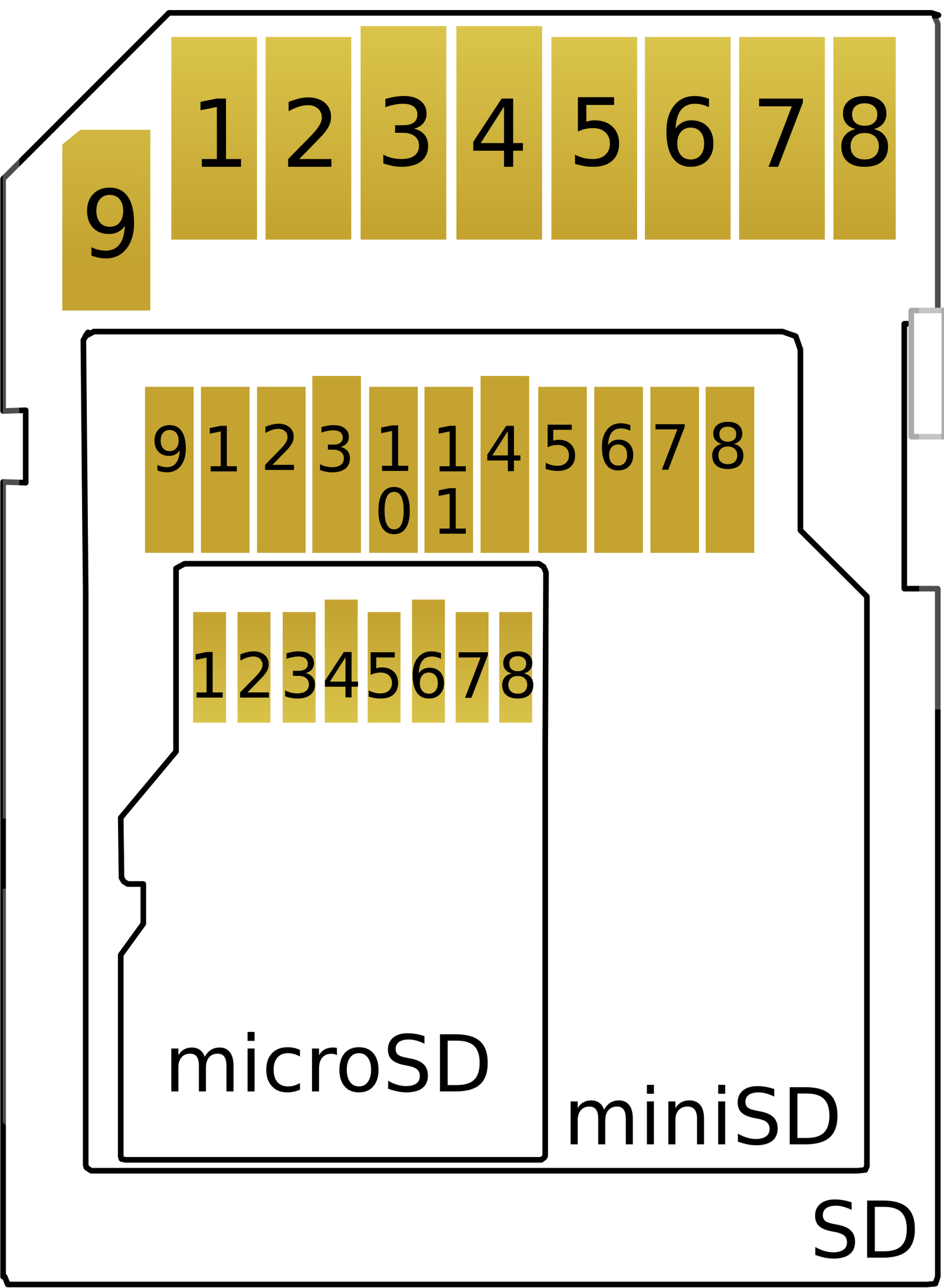
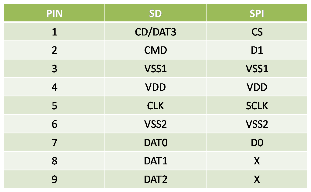
SD Bill of fare pinout
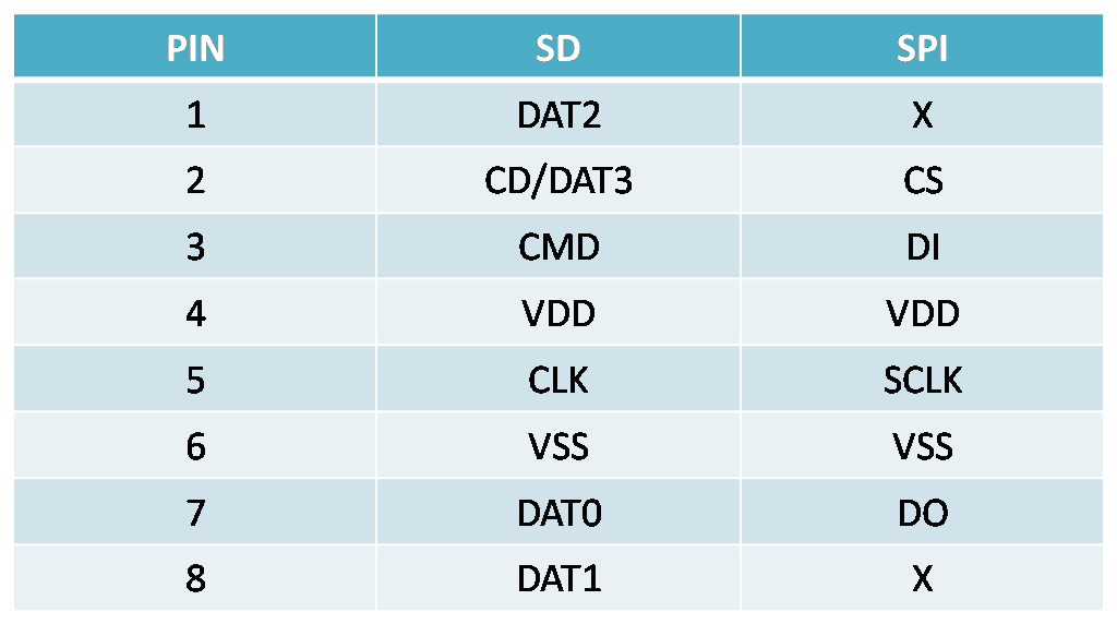
MicroSD Card pinout
Most micro-controllers use the SPI communication protocol to interface with the SD cards. The SD cards have a microcontroller that shows their availability to the master controller(microcontroller). The micro-controller sees the SD card as an addressable sector on which read/write functions are possible. Once the microcontroller is in the SPI manner, communication between the chief and the slave is done via four pins viz. clock, bit select, information in and information out. It should be kept in mind that throughout the communication between the ii devices, the micro-controller will be sending out the clock.
Most development boards have a defended SD carte du jour slot. But to empathize the connections, allow u.s.a. analyze this fairly simple circuit.
Circuit
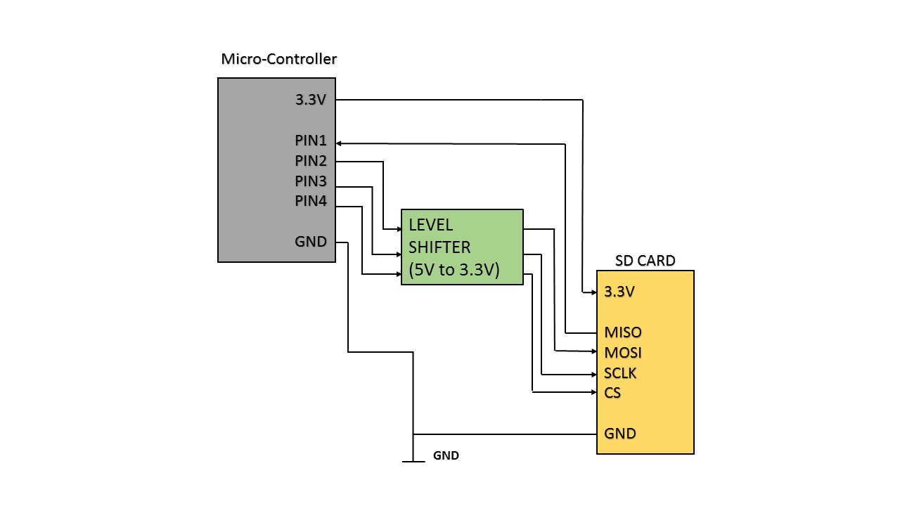
If the logic level of the microcontroller is different than the SD menu, level shifter needs to be used for converting the line voltages.
The MISO (master in serial out) pin should exist connected to the SDI (series data in) pin on the microcontroller.
The MOSI (principal out serial in) pin should be continued to the SDO (serial data out) pin on the microcontroller.
The SCK (series clock) pin should be connected to the SCK (serial clock) pin on the microcontroller.
The CS (chip select) pin should be connected to the corresponding CS pin on the microcontroller or on whatsoever digital I/O pivot on the microcontroller. A common ground is provided.
Of import Note: While connecting the power supply, brand sure that the supply is drawn from a iii.3V supply as a 5V supply would see your carte go upwardly in smoke.
Interfacing
One time the connections are set, nosotros are set to interface our hardware with the software.
Gear up the directions of each of the iv pins correctly. While activating the SPI mode, an platonic configuration should be, fashion(0,0) and the phase with input sampled at the middle of information out. Likewise, the clock frequency should exist fix in the range of 100 kHz and 400 kHz prior to initializing the carte. Once the initialization is washed, the clock can exist set to a more desired frequency.
SD Commands
Next comes the catchy part, initializing the SD menu and performing the raw data communication. A systematic approach to programming the software would make the task pretty easy.
Only first, it is important to learn how the micro-controller activates the SD card. In that location are a fixed set of commands and responses, which must exist followed to create a command to response structure in our program. The data is transmitted in a byte-oriented format with a definite length.
The following table shows the necessary commands to the card and the corresponding response from the card.
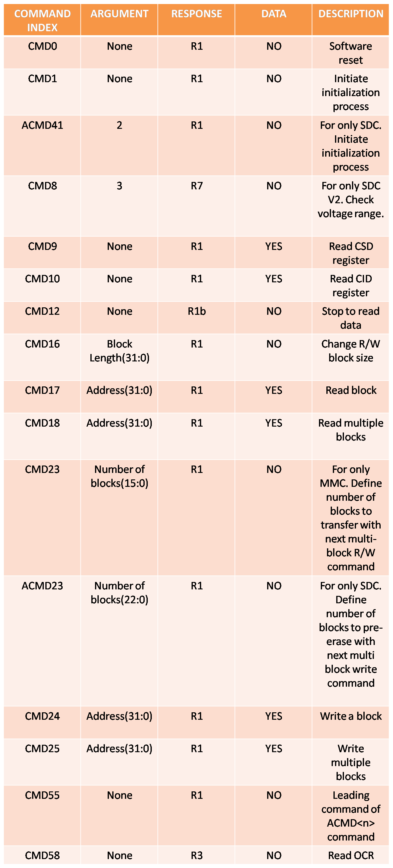
Every command has a constant length of half dozen bytes.
The first byte is the add-on of the control number and the number 64.
Example:
For CMD0: command number 0 + 64 = 64 = 0x40 in hexadecimal.
For CMD1: control number 1 + 64 = 65 = 0x41 in hexadecimal.
And then on.
This is followed by a set of four bytes which are known as the arguments. These arguments usually contain the address of a data or the length of a cake.
The last byte is the CRC (Cyclic Redundancy Cheque) Byte. Most commands in the SPI mode does not require a bank check byte if the CRC feature isn't enabled. For some commands like CMD0, the CRC is 0x95 and in near cases, a 0xFF is sent. Enabling the CRC requires you to send the correct check byte from the micro-controller. So, ensure whether the CRC feature is enabled or disabled.
A command frame looks like this-
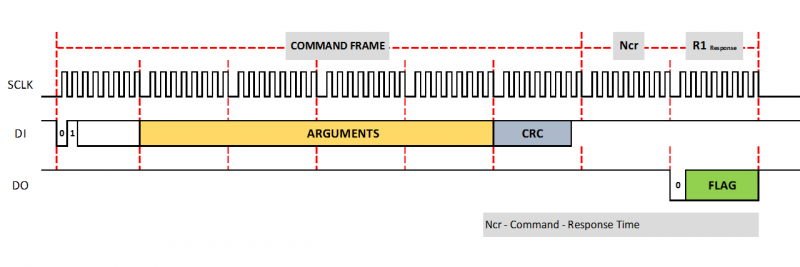
The menu will receive a control when the DO pin (Data Out) is driven high as shown above. The CS pin (Flake Select) must be driven loftier to low before sending the control and must be kept low during the procedure. The time between a control and its response is known as the command response fourth dimension (NCR). Every bit mentioned earlier, regarding the clock pulses from the micro-controller, the corresponding response byte sent back from the card to the microcontroller should be driven by the series clock pulses of the micro-controller. There is a chance that the response byte from the card might become skipped by the microcontroller due to the absence of a driving clock pulse. Hence it is necessary to make sure that an 8-Scrap clock pulse is sent to the Card shortly after the Command Frame is sent (Refer the TECHNICAL Annotation beneath). Too while receiving a Byte from the card, the DI pin (Data In) must be driven high.
Furthermore, let us analyze the different types of responses that nosotros get from the menu and what they hateful.

An R1 response, 0x01 means that the control sent prior to the response has resulted in the card going into an idle state.
A response byte 0x00 means that the command has been accepted and the card volition exist waiting for the proposed consequence to take place. If any other $.25 in an R1 response is set, it is the outcome of an fault and it'll be down to the factor mentioned in each R1 response flake in the figure.
Initializing the SD Bill of fare
At present, as far as sending the commands are concerned, there is an order in which they must be sent. Only the commands, CMD0, CMD1, ACMD41, CMD58 and CMD59 volition be accepted when the card is in its idle state. Sending whatsoever other control will probable to yield an illegal response.
TECHNICAL NOTE: After interfacing the card, the micro-controller must always ship a set up of bytes, which we will refer to every bit dummy bytes. One dummy byte is 0xFF. These dummy bytes have a elementary yet significant purpose. Prior to the initialization, the card must know the frequency at which the information is beingness sent. Past sending around 75 dummy $.25 approximately (dummy byte * x times = 80 bits), the carte du jour will be ready for communication. Likewise even later every command is sent, it is a skilful practice to send at least one dummy byte. A logical explanation for this is that advice is driven by the clock pulse of the micro-controller. The clock pulse is sent just when the information buffer is filled. Subsequently every response is sent and prior to the next command or between command and response, the SCK will stop generating pulses due to an empty data buffer. To ensure the continual transmission of clock pulses between every command, make full the data buffer with a junk value such as a dummy byte. To create a dummy byte function with the number of loops as the argument.
The starting time control to be sent to the card is the CMD0 command. The structure of every other control-response should exist based on this model.
- Drive the Practice pin high.
- Bulldoze the CS pin from high to depression.
- Send a dummy byte.
- Then send the following 6-byte command continuously
Get-go byte: 0x40
Next iv bytes: 0x00000000
CRC byte: 0x95
- Send another dummy byte or every bit many as required, to generate the SCK giving fourth dimension for the SD card to reply to the command request.
- Look for the receive flag bit to fix and so read the response from the SD carte or create a loop to read the response a few number of times. The response should reach dorsum within the command to response (Ncr) time. Or else, something must be wrong.
- The desired response is 0x01, significant the card is in the idle state and nosotros are good to go.
Send the CMD8 command next to check the version of your SD menu.
The difference in the half-dozen-byte commands are
Beginning byte: 0x48
Next four bytes: 0x000001AA
CRC byte: 0x87
Nosotros are looking for two possibilities in our response byte. Either 0x01 or 0x05.
A 0x01 response means that you accept a version ii SD card. The 0x01 response is followed past the 4 bytes 0x00, 0x00, 0x01, 0xAA in the order of their transmission from the SD card which is, in fact, the statement y'all transport in your command.
If the response is 0x05, it means the menu is a version 1 or an MMC carte. If the carte is actually a version ii SD card, then this response is the upshot of an illegal command. Likewise, the carte is now in the idle land.
One time the to a higher place ii commands (CMD0 and CMD8) are washed, it is safe to say that our SD Card is working in skillful condition and ready for data Read/Write.
Additionally, simply to ensure whether the SD Carte du jour is functioning in the right working voltage, send the CMD58 Command.
Next, we must initiate the initialization process. For this send a CMD1 command and expect for response 0x00, meaning the idle state bit is cleared.
If yous are using an SDC or for the purpose of creating a general code, it is advisable to send an ACMD41 command first to begin the initialization procedure and so send the CMD1 control if the ACMD41 is rejected.
Either way, the initialization procedure might take a few hundred milliseconds, so iterating a few number of times to bank check for the response byte would be advisable.
Suppose the response of CMD8 resulted in 0x05, a few considerations have to be made regarding the initialization process. Version i cards may non support the ACMD41 command. And fifty-fifty if they practise support the ACMD41 command, send the CMD55 command and bank check for the response, which will be 0x05 instead of 0x01 so instead of sending the CMD41 command, ship a CMD1 command to complete the initialization procedure.
Read/Write SD Card
Now, we are ready for the raw data read/write.
The get-go matter to do here is to ready the block size of the read/write block.
For this, send CMD16 command. The arguments for this command should specify the block length.
Example: To set the block length to 512 bytes, send the 4-byte argument as 0x00000200.
Send a 0xFF as the CRC byte and wait for a 0x00 response byte.
Regarding the commands for the read/write, the full general construction for sending the commands is the aforementioned, but with a few additional details too.
The iv-byte statement of every command will contain the specified accost of the sector from where the data is existence read or written to.
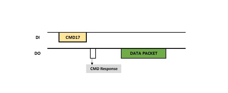
Transport the CMD17 command for a southingle read cake and wait for the expected response 0x00. Once that is done, wait for the SD bill of fare to send another response, 0xFE. This response, transmitted by the SD card, is an indication for the start of continuous manual of a block of data. At the finish of this, transport a dummy byte or ii and the process is complete.
Unmarried Cake Read Timing Diagram
Multi-Block Read Timing Diagram
In the case of CMD18 for a multi-read block, follow the process up until the 0xFE response. After this, the menu will be transmitting blocks of data till it receives a CMD12 command, which is the indication from the microcontroller that the block read is over.
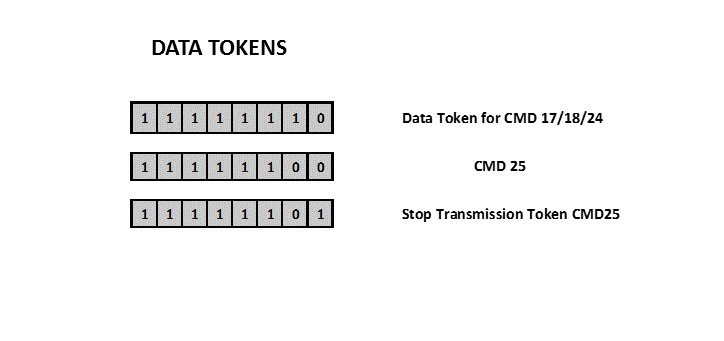
In case of performing a unmarried block write or a multi-cake write, transport CMD24 or CMD25 respectively and await for the response 0x00. Every cake write requires a start token 0xFE in case of a single block write and 0xFC in case of a multi-block write to enable the card to commencement writing a single cake of information onto the specified sector. Ensure 0xFC is sent for every block-write during a multi-block write. After every block writes, a finish token 0xFD must be issued (not required in the example of single block write). After the completion of all the data block write, a CMD13 command is mandatory.
Exercise non forget to ship dummy bytes between responses as well as prior to sending kickoff tokens.
Unmarried Block Write Timing Diagram
Multi-Block Write Timing Diagram
Interfacing Microcontrollers with SD Card – Menses diagram
Creating a office for each of the read/write sections is the ideal fashion to code the software. This is the basic structure to be followed during read/write operations performed on raw information on an SD menu.
Farther reading
- Raw SD Read/Write Using PIC18F4550
- SD Bill of fare Using Petit File Arrangement
Source: https://openlabpro.com/guide/interfacing-microcontrollers-with-sd-card/
0 Response to "Device to Read Micro Sd Card Circuit"
Post a Comment